
Company News
Company News
What are the core technological challenges of IC carrier boards?
Author:RUNMTEK
Publication Date:2026-01-07
Page Views:36
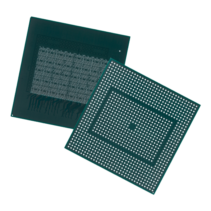
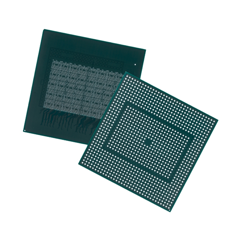
As the core carrier of advanced packaging, the IC carrier board's core process difficulties are concentrated in three dimensions: high-precision manufacturing, material adaptability, and yield control. These difficulties are specifically reflected in the following key aspects:
Ultra-fine circuit and micro-via processing
Advanced packaging demands extremely high precision for the line width/space (L/S) of IC carrier boards. Carrier boards for 5G and AI chips often require L/S to be no greater than 20/20μm, and some high-end products even demand values below 10/10μm. Traditional mechanical drilling and wet etching methods are no longer sufficient to meet these precision requirements, necessitating the adoption of technologies such as laser direct imaging (LDI), plasma etching, and laser drilling.
The difficulties lie in the fact that energy control in laser processing is challenging, prone to issues such as burrs at the edge of the circuit and uneven micro-hole diameters. Additionally, ultra-fine circuits require stringent alignment accuracy (with positional errors controlled within ±2μm), and layer misalignment during the lamination of multi-layer boards can directly lead to failure.

Lamination and warpage control of ultra-thin substrates
To accommodate the demand for miniaturized and thinner chips, the substrate thickness of IC carriers continues to decrease (with some products having a thickness of less than 0.1mm). The lamination process for multi-layer carriers requires precise bonding of the core board and prepreg (PP) under high temperature and pressure.
The difficulty lies in the fact that ultra-thin substrates are prone to warping and deformation during the hot pressing process. Moreover, the significant differences in the coefficient of thermal expansion (CTE) among different materials (such as epoxy resin, BT resin, PI) can lead to interlayer stress concentration, resulting in defects such as delamination and cracking. Additionally, thin substrates are prone to damage during handling and processing, which places extremely high precision requirements on the automation equipment of the production line.
Surface treatment and reliability assurance
The surface of the IC carrier board needs to undergo treatments such as electroless nickel-gold (ENIG), organic solderability preservative (OSP), and electroless palladium-nickel-gold (ENEPIG) plating to ensure the adhesion and corrosion resistance of chip soldering.
The difficulty lies in the poor uniformity of surface treatment for ultra-fine circuits, which is prone to insufficient or excessive thickness of local plating layers. At the same time, the carrier board needs to meet reliability tests such as high temperature and high humidity (HTHS) and thermal shock, and insufficient bonding between the plating layer and the substrate can lead to solder joint failure. This places extremely high demands on the parameter control of the electroplating process (current density, temperature, pH value).
Material selection and adaptability challenges
Different application scenarios have significant differences in performance requirements for IC carrier boards: high-frequency communication chips require carrier boards with low dielectric constant (Dk) and low dielectric loss (Df); automotive chips require carrier boards with high heat resistance and high mechanical strength; consumer electronics chips require low cost and thinness.
The difficulty lies in the fact that it is difficult for a single material to meet all performance requirements. For example, the dielectric properties of traditional BT resin cannot meet high-frequency requirements, while PTFE materials with low Dk/Df are difficult and costly to process. At the same time, new materials have poor compatibility with existing processes, requiring readjustment of parameters in etching, electroplating, lamination, and other steps, leading to a long research and development cycle.
Cost balance under high yield rate
The equipment investment for the aforementioned high-precision processes (such as LDI equipment, laser drilling machines) is costly, and the yield control for ultra-fine manufacturing processes is challenging - issues such as circuit defects, layer misalignment, and micro-via blockage can all lead to product scrap.
The difficulty lies in the fact that every 1 percentage point increase in the yield of high-end IC carrier boards requires significant investment in process debugging and testing. However, the downstream market is cost-sensitive. How to control production costs while meeting high-precision requirements is the core challenge that restricts corporate profitability.
Hot News
-
 What exactly is the integration of hardware and software? Why are more and more products relying on it?2026-01-07
 -
 How can we overcome the difficulties in the window-opening process of soft-hard composite boards?2026-01-07
 -
 What are the benefits of prototyping and sample making for automotive circuit boards?2026-01-07
 -
 What are the core technological challenges of IC carrier boards?2026-01-07