
Industry Trends
Industry Trends
What are the benefits of prototyping and sample making for automotive circuit boards?
Author:RUNMTEK
Publication Date:2026-01-07
Page Views:32
Reduce the cost and loss of small batch sampling
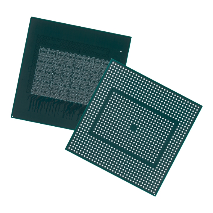
Automotive PCBs have stringent requirements for base materials (such as high Tg FR-4, halogen-free materials) and processes (such as thick copper, impedance control). When prototyping a single board, the fixed costs of equipment debugging, material cutting, and processing account for a significantly high proportion.
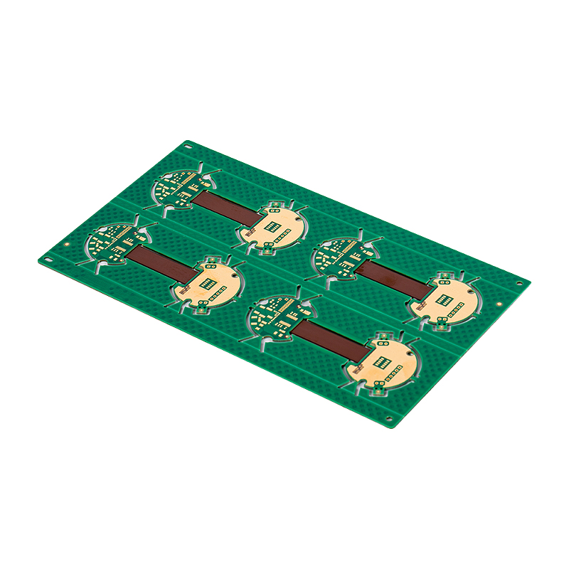
Panel proofing allows multiple identical or different automotive circuit boards (such as body control boards and headlight driver boards) to be integrated and processed on the same substrate, spreading the fixed costs of cutting, drilling, exposure, and other processes, significantly reducing the proofing cost of individual boards. At the same time, it reduces the waste of substrate scraps, especially for high-cost substrates such as thick copper and high-frequency materials commonly used in automotive boards.
Improve sampling efficiency and shorten R&D cycle
During the research and development phase of in-vehicle electronics, frequent iteration of design schemes is required. Panel prototyping can complete the processing of multiple samples or multiple pieces of the same type of sample at once, eliminating the need for multiple rounds of equipment debugging on the machine.
For example, when prototyping a PCB for an automotive radar, 5-10 boards can be grouped together for processing, which can save more than 60% of processing time compared to multiple single-board prototyping. Additionally, panel processing reduces the frequency of equipment changeovers and parameter adjustments, thereby minimizing the risk of process deviations caused by repeated debugging and speeding up sample delivery and subsequent testing progress.
Ensure the process consistency of the samples to meet the high reliability requirements for in-vehicle applications
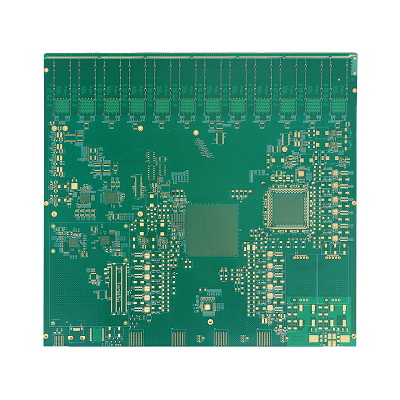
The requirements for impedance stability, copper thickness uniformity, and interlayer alignment accuracy in automotive circuit boards are significantly higher than those in consumer electronics. During panel assembly and proofing, all samples on the same substrate are processed in an identical environment (with consistent temperature, pressure, and etching parameters), ensuring maximum process consistency among the samples.
This consistency can avoid parameter fluctuations caused by the separate processing of individual boards, allowing R&D personnel to more accurately verify the reliability of design schemes. For example, in high and low temperature cycle testing, it can eliminate the interference of process differences on test results.
Facilitate integrated testing and reduce testing tooling costs
The testing of on-board PCBs requires coverage of multiple aspects, including functional testing and reliability testing (such as thermal shock, damp heat aging). Samples in panel assembly can share a set of testing fixtures.
For example, panel samples can be directly fixed on a test frame for batch power-on testing, eliminating the need to individually customize fixtures for individual small boards, thus saving tooling development costs. At the same time, the rigidity of the panel is stronger, making it less prone to deformation during testing due to clamping and handling, thus avoiding test misjudgments caused by substrate deformation.
Reduce the difficulty of transitioning to small-batch trial production
During the transition phase of in-vehicle PCBs from prototyping to small-batch trial production, the panel assembly scheme can be directly applied to the initial mass production line.
R&D personnel can optimize the panel layout (such as adjusting panel spacing and optimizing process edge design) for the mass production stage in advance based on the yield data from panel proofing, reducing the process transfer cost from proofing to mass production. At the same time, the process parameters for panel processing (such as drilling compensation and etching factors) can be directly migrated to the mass production line, reducing the risk of yield fluctuation in mass production.
Hot News
-
 What are the differences between rigid-flex PCBs and FPCs? Don’t mix them up anymore!2026-01-07
 -
 How can the interlayer bonding strength of rigid-flex boards be ensured?2026-01-07
 -
 What technical challenges does the localization substitution of PCB circuit boards face?2026-01-07
 -
 What are the key design points for biocompatibility in medical-grade circuit boards?2026-01-07